-->

WORKING OF 74HC138 IC

By
Working of  74HC138 IC


               74HC138 is a decoder of the type octal 3- to- 8 Line Decoder / Demulator and Inverter.
The chip enables 3 pins - A, B and C - to output 8-bit , meaning that decodes three address lines in 8 possible ways . Simple, with 3 input bits to form 8 Address : 2 3 = 8; See the truth table:


An address decoder is also called a " demultiplexer " or " demux " . Although these terms are more generic and can refer to devices other than decoders addresses, TTL 74138 mentioned here can be called " demux 3- to -8" .
Decoders addresses are fundamental building blocks for systems using bus bars. They are represented in all families of integrated circuits and all the standard libraries FPGA and ASIC . They are discussed in introductory texts in digital logic design


Making multiple input by 3 wire Interfacing .

By
Parallel to serial  Interfacing with Micro controller 

Interfacing with 74HC165 with 8051


   I am trying to make multiple input with using minimum input port of micro controller ,ie 3 wire .
By using a 3 wire we can interface more input as we wish.


 I am making a tutorial for it , Basics of 74HC165  which is a parallel to serial shift register .


Only three pin is connected with this IC . 
1)   SH/LD  or PL  is used load  parallel data to the IC .A low pulse (ground) is applied for store the         parallel data at the pin from A to H . And a High (5 Volt) is applied to stop the reading from the          PIN A to H .
2) Then to read the loaded or saved data to Micro controller we have to give clock to the PIN 2 of           74HC165  (CLK) . 8 pulses is applied to read 8 bit (Pin A to B)

3) QH / SO . serial out pin is used to get the stored parallel data to serially.

The CLK INH pin must be connect in ground for enable clock.


    To use cascaded 74HC165 for increasing i/p .connect the Seriall output pin (PIN 9) of first satge into serial input of first stage see the following circuit.


see the code below


  #include  
#include
#include "lcd.h"
sbit PL = P1^0; // Loading parallel data to HC165.
sbit CLK = P1^1; // Clock pulse to HC165.
sbit Beep = P1^2; //
sbit data_in = P1^3;

void clock(void);
void display(unsigned char value);

void main()
{
unsigned char position ,no_of_ip = 17;
lcd_init();
string(" gElectron");
while(1)

{
PL = 0 ;
delay(2);
PL = 1;

for(position = 1; no_of_ip > position; position++ , clock())
{

if(data_in == 1)
display(position);

}
}
}

void clock(void)
{
CLK = 1;
delay(1);
CLK = 0;

}

void display(unsigned int value)
{
unsigned int a[1];
Beep = 1;
lcd_init();
lcd_cmd(0x01);
string("Pressed key ");
lcd_cmd(0xc0);
sprintf(a,"%d",value);
string(a);
delay(1);
Beep = 0;

}

Download the whle file here github.


Making multiple input by 3 wire Interfacing .

By
Parallel to serial  Interfacing with Micro controller 

Interfacing with 74HC165 with 8051


   I am trying to make multiple input with using minimum input port of micro controller ,ie 3 wire .
By using a 3 wire we can interface more input as we wish.


 I am making a tutorial for it , Basics of 74HC165  which is a parallel to serial shift register .


Only three pin is connected with this IC . 
1)   SH/LD  or PL  is used load  parallel data to the IC .A low pulse (ground) is applied for store the         parallel data at the pin from A to H . And a High (5 Volt) is applied to stop the reading from the          PIN A to H .
2) Then to read the loaded or saved data to Micro controller we have to give clock to the PIN 2 of           74HC165  (CLK) . 8 pulses is applied to read 8 bit (Pin A to B)

3) QH / SO . serial out pin is used to get the stored parallel data to serially.

The CLK INH pin must be connect in ground for enable clock.


    To use cascaded 74HC165 for increasing i/p .connect the Seriall output pin (PIN 9) of first satge into serial input of first stage see the following circuit.


see the code below


  #include  
#include
#include "lcd.h"  
sbit PL  = P1^0;   // Loading parallel data to HC165.
sbit CLK = P1^1;   // Clock pulse to HC165.
sbit Beep  = P1^2;   // 
sbit data_in  = P1^3;

  void clock(void);
  void display(unsigned char value);
     
void main()
{  
 unsigned char position ,no_of_ip = 17;
  lcd_init();
  string("   gElectron");     
  while(1)

   {  
      PL = 0 ;
  delay(2);
  PL = 1;

   for(position = 1; no_of_ip > position; position++ , clock())
  {     
  
    if(data_in == 1)
     display(position);   

  }
   } 
}  

 void clock(void)
 {
   CLK = 1;
   delay(1);
   CLK = 0;

 }

void display(unsigned int value)
  {  
  unsigned int a[1];
    Beep =   1;
    lcd_init();
 lcd_cmd(0x01);   
    string("Pressed key ");
    lcd_cmd(0xc0); 
  sprintf(a,"%d",value);  
     string(a); 
     delay(1);
     Beep = 0;
     
  }   


Download the whle file here github.


Google Photo Backup

By


        Google lunched a New application called Google photos   where we can add our lime time photos with each album with geo tagging location . google app automatically upload the photos and with our location . So we can see the photos including the location where was the photo taken .
The great advantage is that who is suffering with low memory mobile ,but they need to upload their photos accordingly , use the Google photo application sync with it. After syncing the photos we can delete the photos from the mobile .It delete only from the mobile and available on the net ever .


* It can easily share on social network
* It can be see Monthly view ,day view and more


 A geotaging location shown in the album cover . The photos automatically created while travelling.and tagged with the location


Microcontroller Based ammeter and voltmeter using Atmega 16

By
Here  Atmega16  measuring the  current and voltage by inbuilt comparator  .Previous post described how to read ADC value click here . Two  ADC port is used  PA0/ADC0  is  measuring voltage .And PA1/ADC1 is  measuring current .

For Advancedtutorials click here Voltmeter Design

                We have to measure 0 to 12 volt, but controller can only read as maximum voltage 5 volt .
Hence a voltage divider circuit used to reduce the corresponding voltage level  at a mximum 5Volt.


take
Vin  = 12volt
Vout = 5 volt.
Assume one of the resistor value and find out the other .
***********************************************************************************
  we have to measure current ,But we cant directly measure the current . there are more technique to measure the current. we uses a shunt resistor method .
The millivoltmeter voltage is taken and calculated by some equation and displayed as current .for more click here

For example .
According Ohm's law,  0.1 Ohm resistor under 1A current will give 0.1V voltage drop
*********************************************************************************


                                             The program shown below
* Created: 14-Oct-15 6:44:15 PM
* Author: Gireesh
*/
#define F_CPU 16000000UL
#include <avr/io.h>
#include<util/delay.h>
#include"lcd.h"
#include "adc.h"

int main(void)

{

unsigned char volt[5] ,current[5];
DDRD = 0xFF;
int v,i;
char ch_sec =0;
adc_init();
lcd_init();
string ("G Electron ");
LINE2
string("Power Supply");
_delay_ms(50);
CLEAR
while(1)

{
v = read_adc(0); // reading voltage
i = read_adc(1); // reading voltage for current
v = (v * 4.89 * 2.4)/10;
i = (i * 2.92);
i = ((i*4.89)/0.47)/10;


if(v< 1200)
{
volt[0] = ((v /1000)%10)+0x30;
volt[1] = ((v /100) % 10) + 0x30;
volt[2] = '.';
volt[3] = ((v/ 10) %10) + 0x30;
volt[4] = (v % 10) + 0x30 ;


string("Volt : ");
for(int i =0; i<5;i++)
lcd_data(volt[i]); // just displaying ADC value
string("V");
}
else
{

string("Over Voltage");
}
LINE2
if(i<3100)
{
current[0] =((i /1000)%10)+0x30;
current[1] = '.';
current[2] = ((i /100) % 10) + 0x30;
current[3] = ((i/ 10) %10) + 0x30;
string("Current : ");
for(int i =0; i<4;i++)
lcd_data(current[i]);
string("A");
}
else
{

string("Over Current");
}
_delay_ms(50);
CLEAR
}
}
design circuits to feed controller for current and Volt. the whole project can be download Below including proteus file For downloading click below
      
                                                 Download

Microcontroller Based ammeter and voltmeter using Atmega 16

By
Here  Atmega16  measuring the  current and voltage by inbuilt comparator  .Previous post described how to read ADC value click here . Two  ADC port is used  PA0/ADC0  is  measuring voltage .And PA1/ADC1 is  measuring current .

For Advancedtutorials click here Voltmeter Design

                We have to measure 0 to 12 volt, but controller can only read as maximum voltage 5 volt .
Hence a voltage divider circuit used to reduce the corresponding voltage level  at a mximum 5Volt.


take
Vin  = 12volt
Vout = 5 volt.
Assume one of the resistor value and find out the other .
***********************************************************************************
  we have to measure current ,But we cant directly measure the current . there are more technique to measure the current. we uses a shunt resistor method .
The millivoltmeter voltage is taken and calculated by some equation and displayed as current .for more click here

For example .
According Ohm's law,  0.1 Ohm resistor under 1A current will give 0.1V voltage drop
*********************************************************************************


                                             The program shown below
* Created: 14-Oct-15 6:44:15 PM
 *  Author: Gireesh 
 */ 
#define F_CPU 16000000UL
#include <avr/io.h>
#include<util/delay.h>
#include"lcd.h"
#include "adc.h"

int main(void)
  
{   
 
 unsigned char volt[5] ,current[5];
   DDRD = 0xFF;
   int v,i;
   char ch_sec =0;
    adc_init();
    lcd_init(); 
 string ("G Electron ");
 LINE2
 string("Power Supply");
 _delay_ms(50);
 CLEAR
 while(1)
 
 {
   v =   read_adc(0);  // reading voltage    
   i =   read_adc(1);  // reading voltage for current  
   v = (v * 4.89 * 2.4)/10;
   i = (i * 2.92);
   i = ((i*4.89)/0.47)/10;


   if(v< 1200)
   {
   volt[0] = ((v /1000)%10)+0x30;
   volt[1] = ((v /100) % 10) + 0x30;
   volt[2] = '.';
   volt[3] = ((v/ 10) %10) + 0x30;
   volt[4] = (v % 10) + 0x30 ;
   
   
   string("Volt    : ");
   for(int i =0; i<5;i++)
  lcd_data(volt[i]); // just displaying ADC value 
  string("V");
  }
  else
  {
 
   string("Over Voltage");
    }
 LINE2
 if(i<3100)
 {
 current[0] =((i /1000)%10)+0x30;
 current[1] = '.';
 current[2] = ((i /100) % 10) + 0x30;
 current[3] = ((i/ 10) %10) + 0x30;
 string("Current : ");
 for(int i =0; i<4;i++)
 lcd_data(current[i]);
 string("A");
 } 
 else
 {
  
  string("Over Current");
 }
 _delay_ms(50);
 CLEAR 
 }  
}
design circuits to feed controller for current and Volt. the whole project can be download Below including proteus file For downloading click below
      
                                                 Download

ADC Reading With Internal Adc Of AVR - Atemga 32 And Displaying On LCD

By

Download HereADC Reading With Internal Adc Of  AVR - Atemga 32 And Displaying On LCD

According to data sheet there are 3 registers are used to works the ADC in AVR atmega 32 
ie , 

1) ADMUX
2)ADSCR
3)ADC


1) ADMUX :-

 It is an 8 bit Register ,each bit has some functions as follows 

REFS1 & REFS0 :- is used for the reference Voltage  with respect to our analog input (for resolution)  to know more search this blog.
I am giving 5volt as reference so selected REFS1 = 0 & REFS0 = 1

ADMUX=(1<<REFS0); // AVcc with external capacitor at AREF  ,giving a high to REFS0.

MUX0-MUX4  :- it is used to select the input channel ,ie 8  analog input channel can be given so desired one selection by giving appropriate value .
  ADLAR : - used to shift the resulted data (ADC Value) left or right .I am using right shift so makes as low.
.....................................................................................................................................

2) ADSCR :-  ADCSRA = (1<<ADEN)|(1<<ADPS2)|(1<<ADPS1)|(1<<ADPS0);

It is also an 8 bit register .

Bit 7 used to ADC ON (ADC Turn ONing by applying a high bit )
Bit6 ADSC is used to start the conversion .and still maintain it value as high  up to the conversion . after conversion it becomes low (Zero)
ADATE and ADIF is not used by me now .(not by using Intruppet
Bit 0 to bit2  is used for select ADC frequency . 

\
2) ADC: It is a 16 bit to 8 bit register ADCL & ADCH. By applying right shift value it is autmatically set as normal value so we can take simple value from it

 eg :  return (ADC);
 adc_value = read_adc(ch_sec); 

The program as follows . The full program can be download below including Proteus simulation file.


ADC reading with Internal adc of PIC16F77 and displaying on LCD

By
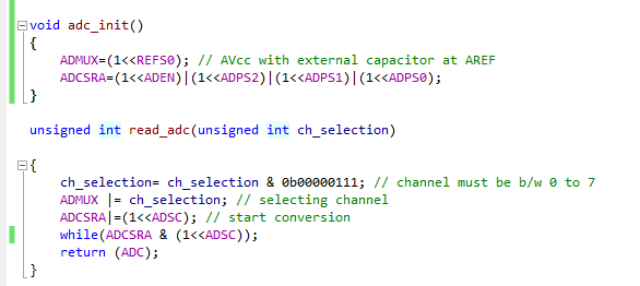
In PIC16F877 has 8 channels are available for adc input ie AN0 to AN7.Any one can be use ,we can select the the channel by selecting channel selection bit.

The Whole project Can be download at the Bottom of the post .


            In ADC the Vref voltage is important in accuracy of the ADC conversion.Low Vref gets more accuracy . But This PIC has a 10 bit result ion so it is enough As follows some example

If    Vref             =    4.096 volt
     Bit resolution  = 8 ie 2^8 =256
then  4.096/256 = 16Millvolt Per Bit
        3.88/256 = 15mv/bit
        2.56/256 = 10mv/bit
giving vcc as vref (5Volt) in 10 bit Resolution
Vref =5 v
Bit resolution  = 10 bit ,ie 2^10 = 1024
so
            5/1024 = 4.8828 millivolt /Bit
Here  taking 5 volt as vref

For getting ADC value the following steps are needed

 * Initialization of ADC
 * Reading ADC value


 Initialization of ADC

 Initialization of ADC mean that
Configure the ADC PORT  for that PIC has 4 registers they are
* ADCON 0
* ADCON 1
* ADRESH
*ADRESL

ADCON0 :- it is an 8 bit register it decide how the ADC worrks in accordance with the following bit have to set .
Lasr(msb bit) two bit decide the clock of the ADC ie the conversion speed.if we select the the main PIC crystal frequency as 20MHz
then I will select the First tw register value is 10
ie 10 = Fosc/32
after calculating the clock speed there must be a time 1.6 micro second for one bit conversion these time is called TAD . So to convert  10 bit  need 10x1.6 microsecond .,Look Data sheet page No .133 Section 11-2.

 I am selecting the ADC clock selection bit is 10

ADCS1  = 1
ADCS0  = 0
ie fosc/32    Look Datasheet Page No. 130 section 11.2

Calculation
            20Mhz/32 = 625000Hz ie 1.6Microsecond
           For one TAD is 1.6 is correct .(Look Data sheet page No .133 Section 11-2)

Then ,
The the 3rd,4the and 5th bit is the analog channel selection Bit from the Port AN0 to AN7.


The second bit(GO/DONE) is used to Start the conversion  of analog value to digital when its value is one .And automatically reset (become zero) whenever the completion take place  

 GO/DONE: A/D Conversion Status bit
When ADON = 1:
1 = A/D conversion in progress (setting this bit starts the A/D conversion which is automatically
cleared by hardware when the A/D conversion is complete)
0 = A/D conversion not in progress  

The Second Bit is not used Leave it as Zero

The First Bit is the Bit to Turn On the ADC .(powering on the ADC).

So the ADCON0 value is 10000001 in Hex a 0x81;

ADCON1 :-


The Bit From Bit 0 to Bit 3  are used decide  to How act the Analog PIN . How the Vref and GND voltage are given. I am selecting the first one
0000 becuase the 8 bit of AN is selected as Analog (denoted above as "A")
And the Vref is taken as VDD ie 5volt (VCC)
* channel selected
So the ADCON1 value is 10000000 in hex format = 0x80;

The Last Bit of ADCON1 is ADFM is used to alignment the result of adc (ie the value )
If its value is One The 10 bit adc value is right alimented
If its value is zero The 10 bit is left aligned

ADRESH :- is the Register (8bit) the result of ADC saved here . Our result is 10 bit if we use 10 bit resolution. But the ADRESH register is 8 bit So the 8 bit of the 10 bit adc result is saved in ADRESH the balance 2 bit is saved in ADRESL .
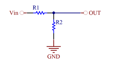


Circuit diagram 


Main Programm
/* 
* File: adc_main.c
* Author: gElectron/Gireesh
*
* Created on September 27, 2015, 6:24 AM
*/


// PIC16F877 Configuration Bit Settings

// 'C' source line config statements

#include
#include"lcd.h"
#include"adc.h"
#include
#define _XTAL_FREQ 20000000 // 20Mh
// #pragma config statements should precede project file includes.
// Use project enums instead of #define for ON and OFF.

// CONFIG
#pragma config FOSC = HS // Oscillator Selection bits (HS oscillator)
#pragma config WDTE = OFF // Watchdog Timer Enable bit (WDT disabled)
#pragma config PWRTE = OFF // Power-up Timer Enable bit (PWRT disabled)
#pragma config CP = OFF // FLASH Program Memory Code Protection bits (Code protection off)
#pragma config BOREN = ON // Brown-out Reset Enable bit (BOR enabled)
#pragma config LVP = OFF // Low Voltage In-Circuit Serial Programming Enable bit (RB3 is digital I/O, HV on MCLR must be used for programming)
#pragma config CPD = OFF // Data EE Memory Code Protection (Code Protection off)
#pragma config WRT = OFF // FLASH Program Memory Write Enable (Unprotected program memory may not be written to by EECON control)


void main()
{
TRISB = 0X00; // output for the 8 bit
TRISA =0XFF;
int adc_value=0x00,ch_sec = 0;
unsigned char digits[5];
lcd_init(); // lcd initialization
adc_init(); // adc initialization
adc_value = read_adc(ch_sec); // reading adc value
string("gElectron ");
LINE2;
digits[0] = adc_value / 1000 + 48;
digits[1] = (adc_value / 100) % 10 + 48;
digits[2] = (adc_value / 10) % 10 + 48;
digits[3] = adc_value % 10 + 48;
digits[4] = '\0';
string(digits);

while(1); // endless loop
}

ADC file
/* 
* File: adc.c
* Author: Krishna
*
* Created on September 27, 2015, 7:14 AM
*/
#include
#include"adc.h"
//#define _XTAL_FREQ 20000000
void adc_init()
{

ADCON0 = 0x81;// 10000001 TAD is fosci/32 and last bit is adc poweron
ADCON1 = 0x80; //all port selected as output ,vref= vcc,
TRISA = 0x2f; //ENANLING AS ANALOG INPUT
TRISE = 0X07; // ENANLING AS ANALOG INPUT
}

unsigned int read_adc(unsigned char ch_selection)
{
if(ch_selection>7) // checking is channel greater than 7
return 0; // yes return zero
__delay_us(50); //adc acquisition time as 19.72 ?s as datasheet
GO_nDONE = 1;
while(GO_nDONE); // after conversion GO_nDONE value become 0 autmatically.
return((ADRESH<<8)+ADRESL);

Downlaod the Whole Project Including Proteus Simulation click heredownload

More Posts

gElectron. Powered by Blogger.

Contributors

16x2 LCD Interfacing with STM32,STM32F103C6

 16x2 LCD  Interfacing with STM32,STM32F103C6 lcd_init(); LCD_LINE1; lcd_String(" GeElectron"); LCD_LINE2; lc...

Contact Form

Name

Email *

Message *

Contact us

Name

Email *

Message *

Follow Us

https://www.facebook.com/gElectron-393939667321867/ FBbox/https://www.facebook.com/IVYthemes

Comments

[blogger]

MKRdezign

Test

Latest

[recent][newsticker]

Technology

Top Ads

RECENT COMMENTS

Subscribe Via Email

Subscribe to our newsletter to get the latest updates to your inbox. ;-)


Your email address is safe with us!

RECENT COMMENTS